Thales Alenia Space in France successfully operates a multi-phase DC-DC converter using SCOPS
SCOPS – 2026, aug 25
After the period dedicated to test setup debugging, Thales Alenia Space in France is pleased to announce three major technical achievements:
1. End-user Test setup validated
The end-user test setup has been successfully validated. It implements a DC-DC converter involving 10 (not yet tested) SCOPS circuits in a multi-phase buck architecture. The setup allows to test up to 200A at output voltages from 0.6V to 1V. The next picture shows the test board:
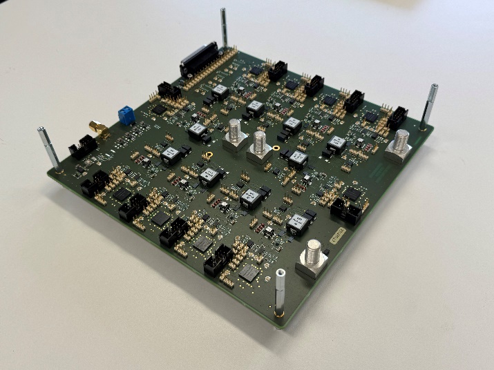
Figure 1: End user test board equipped with 10 SCOPS
2. Synchronization of 8 SCOPS phases (without DCDC operation) achieved with an accuracy of 2 or 3°
The PWM outputs were measured and are shown in the following figure: Dark blue is SCOPS0, light blue is SCOPS1, purple is SCOPS3, green is SCOPS5.
Key observations:
- Two neighboring ICs (SCOPS0 and SCOPS1) show 360/7 degrees phase as expected,
- ICs separated by one SCOPS (SCOPS1/3, SCOPS3/5, SCOPS5/0) show PWM signals spaced by 2×360/7 degrees, as expected.
- No VCO saturation was observed. The PLL operates approximately in the middle of its hold-in range.
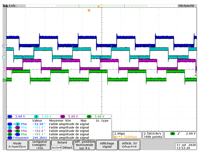
Figure 2: 7 enabled SCOPS PLL lock
3. Buck DC-DC conversion demonstrated in a 5-SCOPS loop at 40A total output current
A buck DC-DC converter was successfully operated using a 5-SCOPS loop with a total output current of 40 A. The maximum current imbalance between phases was 3%, which is comparable to a typical multiphase buck design with current sharing.
Voltages representing the high-side transistors current are observed in the next figure: Light blue is SCOPS1, green is SCOPS2, purple is SCOPS3, dark blue is SCOPS5.
Key observations:
- Two neighboring ICs (SCOPS0 and SCOPS1) show a phase shift of 72 degrees, as expected.
- ICs separated by one SCOPS (SCOPS3/5) show signals spaced by 144 degrees, as expected.
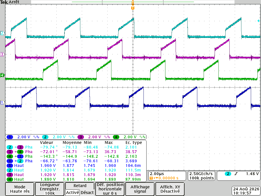
Figure 3: 5 enabled SCOPS in DC-DC converters
- Load steps were also performed in the same configuration. The step goes from 10A to 40A (a lot higher step than specified at system level). This allows assessing the stability and output impedance of the converters. On the next figure, some PWM outs and the output voltage is observed in dark blue.
- For a 10A to 40A load step with a rise time of 2ms, the output voltage behavior implies a 6mOhm output impedance of the converter. It is as expected for low frequency load steps.
- The output voltage behavior shows no overshoot or oscillations which confirms good stability of the voltage loop
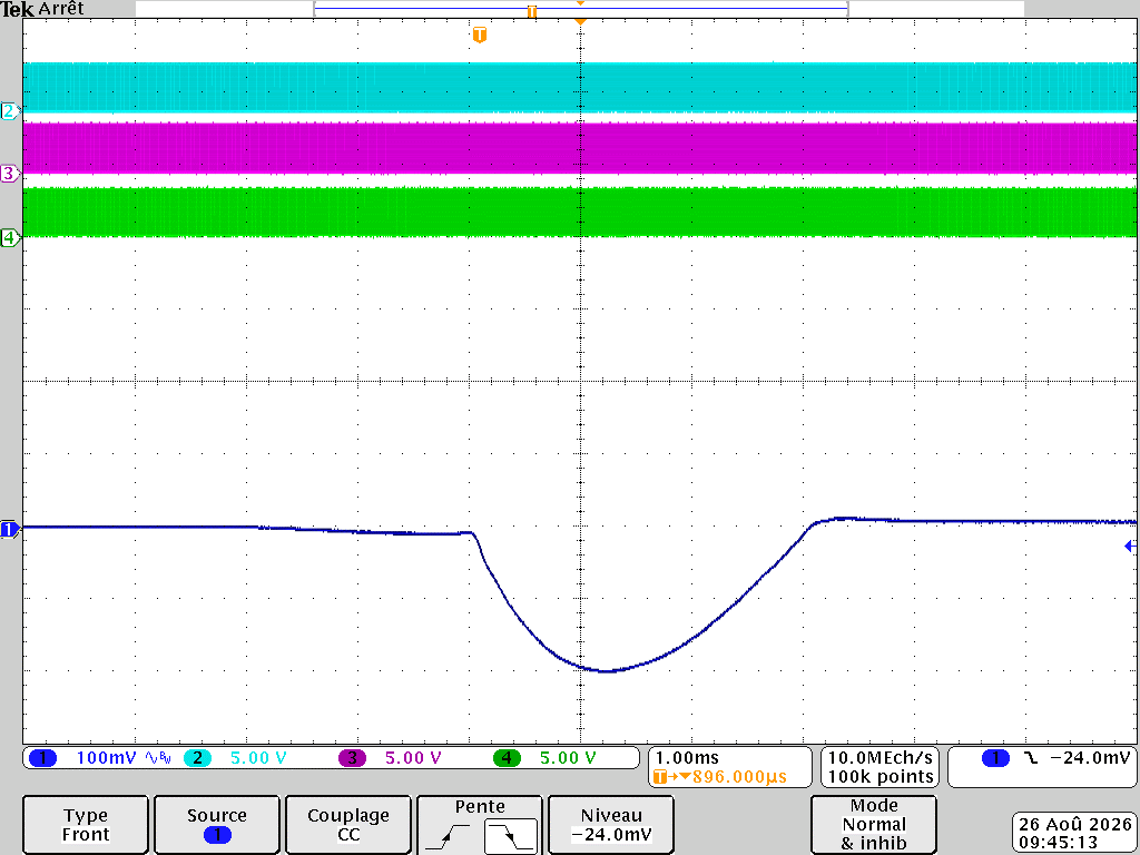
Figure 4: A 10A to 40A loadstep in a 5 SCOPS config
Following this bring-up period, the final test board embedding 10 screened SCOPS devices will be manufactured, validated and submitted to the full end-user test plan over temperature range.
In parallel, ISD Greece & Ireland will perform the screening and unitary validation tests, and Thales Alenia Space in Spain will conduct the radiation tests (SEE and TID) as well as the Life Test.